
This course is based on 14 lectures, 1 lab and some numerical home assigments
No exercises or tutorial will be offered this course round
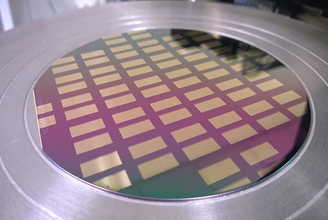
This course is based on the most important component of all integrated circuits, the MOSFET transistor, which is made of silicon with nanometer dimensions. The focus is on low-power CMOS technology. New topologies and manufacturing methods are discussed according to Moore's Law. The course also provides a foundation in silicon-based memory technologies and new alternative technologies based on other physical principles and materials. Components with particularly high performance for e.g. high frequency applications are also introduced with examples from III/V-semiconductor technology or equivalent.
Choose semester and course offering to see current information and more about the course, such as course syllabus, study period, and application information.
KTH Campus
Spring 2027: P4 (7.5 hp)
50%
11666
Normal Daytime
English
Min: 1
Please note: all information from the Course syllabus is available on this page in an accessible format.
Course syllabus IH2663 (Spring 2026–)This course is based on 14 lectures, 1 lab and some numerical home assigments
No exercises or tutorial will be offered this course round
This course is based on the most important component of all integrated circuits, the MOSFET transistor, which is made of silicon with nanometer dimensions. The focus is on low-power CMOS technology. New topologies and manufacturing methods are discussed according to Moore's Law. The course also provides a foundation in silicon-based memory technologies and new alternative technologies based on other physical principles and materials. Components with particularly high performance for e.g. high frequency applications are also introduced with examples from III/V-semiconductor technology or equivalent.
Course contents:
After passing the course, the student should be able to
Knowledge of the function and use of semiconductor components corresponding to 7.5 higher education credits, equivalent to completed course IL2240.
Active participation in a second-cycle course offering where the final examination is not yet reported in LADOK is considered equivalent to completion of the course.
Being registered for a course counts as active participation.
The term 'final examination' encompasses both the regular examination and the first re-examination.
Based on recommendation from KTH’s coordinator for disabilities, the examiner will decide how to adapt an examination for students with documented disability.
The examiner may apply another examination format when re-examining individual students.
If the course is discontinued, students may request to be examined during the following two academic years.
In this course, the EECS code of honor applies, see:
http://www.kth.se/en/eecs/utbildning/hederskodex
IH2663 overlaps to a very large extent with the discontinued course IH2657 and therefore cannot be included in the same degree.