

Apodized waveguide-to-fiber surface grating couplers
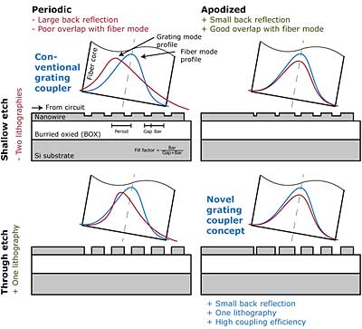
Waveguide-to-fiber surface grating couplers with fill factor apodization offer low back reflection into the silicon waveguide and a single required lithography step. Using through-etched standard silicon-on-insulator (SOI) substrates, it also offers a large process latitude.
Silicon photonics hold great promise for the creation of highly integrated photonic circuits. The high index contrast between silicon and silica permits strong confinement of light, thus enabling small bending radii and strong light-matter interaction. Furthermore, this material choice allows monolithic integration with silicon microelectronics. However, the high effective index and small mode dimensions of single mode silicon waveguides makes fiber coupling challenging.
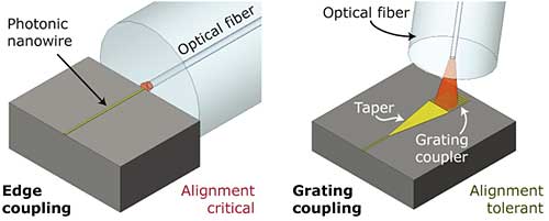
Using surface grating couplers, the mode matching problem can be solved by expanding the width of the on-chip silicon waveguide, and etching a grating into the expanded section that diffracts light out of plane into a fiber placed normal to the surface.
The approach we have taken is to increase the coupling efficiency by tailoring the leakage factor of the grating to the mode profile of the fiber. The main benefits of this approach are a low back reflection into the silicon waveguide and high efficiency in the coupling. With fully etched structures on SOI substrates we also get a single required lithography step and a large process latitude, since the grating depth is defined by an oxide etch stop and not a timed etch.
Example
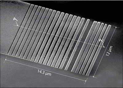
With the grating in the picure we measured a coupling efficiency of 35% on a standard SOI substrate with a 2 μm BOX. We also showed by simulation that with an optimized buried oxide thickness, a coupling efficiency of 72% could be achieved. The imulations show that the apodization process reduces the optical power reflected back into the silicon waveguide from 21% to only 0.1%.
Project members
Mikael Antelius