EDU4Chip
Joint Education for Advanced Chip Design in Europe
Learn chip design by taking an idea all the way to silicon.At KTH, Edu4Chip is integrated into the MSc in Embedded Systems, with a strong focus on embedded electronics, ASIC/FPGA design and a complete hands-on chip design flow from specification to GDSII tape-out.
- Master-level chip design
- Industrial EDA workflows
- 15 ECTS ASIC tape-out project
- European partner network
Edu4Chip within Embedded Systems
Edu4Chip is a Digital Europe project that brings together five European universities to strengthen education in advanced chip design. At KTH, the initiative is embedded in theEmbedded Electronics track of the MSc in Embedded Systems.
The KTH pathway combines digital and analogue foundations with ASIC/FPGA implementation, integrated-circuit design and a project course in which students work through the complete ASIC flow. Students also benefit from Edu4Chip activities across the partner universities, including shared teaching, summer schools and mobility opportunities.
Study pathway: from fundamentals to fabricated hardware
Key KTH courses supporting the Edu4Chip pathway:
| Course | ECTS | Content |
|---|---|---|
| IL2241Introduction to Integrated Circuits | 7.5 | CMOS fundamentals, hierarchical IC design, circuit simulation, physical implementation, verification and industrial EDA tools. |
| IL2225Embedded Hardware Design in ASIC and FPGA | 7.5 | RTL-based hardware design, ASIC/FPGA implementation, synthesis, timing-aware design and verification using modern automated flows. |
| IL2242Analog Integrated Circuits | 7.5 | Core analogue IC concepts including feedback amplifiers, device modelling, noise, distortion, frequency response and analogue layout. |
| IL2243Design of Radio Frequency Integrated Circuits | 7.5 | RF integrated-circuit concepts and building blocks for modern wireless systems. |
| IL2244Project Course in Application Specific Integrated Circuits | 15 | A project-based ASIC course covering the complete flow from specification to submission of GDSII manufacturing masks. Selected designs are fabricated and evaluated. |
A complete ASIC tape-out experience
Students do not stop at RTL or FPGA prototypes. The KTH project course is structured around the real ASIC implementation flow:
- Specification & architecture– define functionality, interfaces and implementation targets.
- RTL & functional verification– develop synthesizable hardware and verify behaviour.
- Synthesis & implementation– map the design to standard cells and build the physical implementation.
- Sign-off– close timing and complete physical verification before release.
- GDSII tape-out– prepare manufacturing data; selected student designs proceed to fabrication.
From prototype to silicon
Before committing a design to silicon, students can validate the system as a working FPGA prototype. The 2026 IL2244 tape-out then took student designs through physical implementation to manufacturable chip layouts.

Prototype first.An IL2244 design demonstrated on FPGA before ASIC tape-out – a concrete way to verify functionality before fabrication.
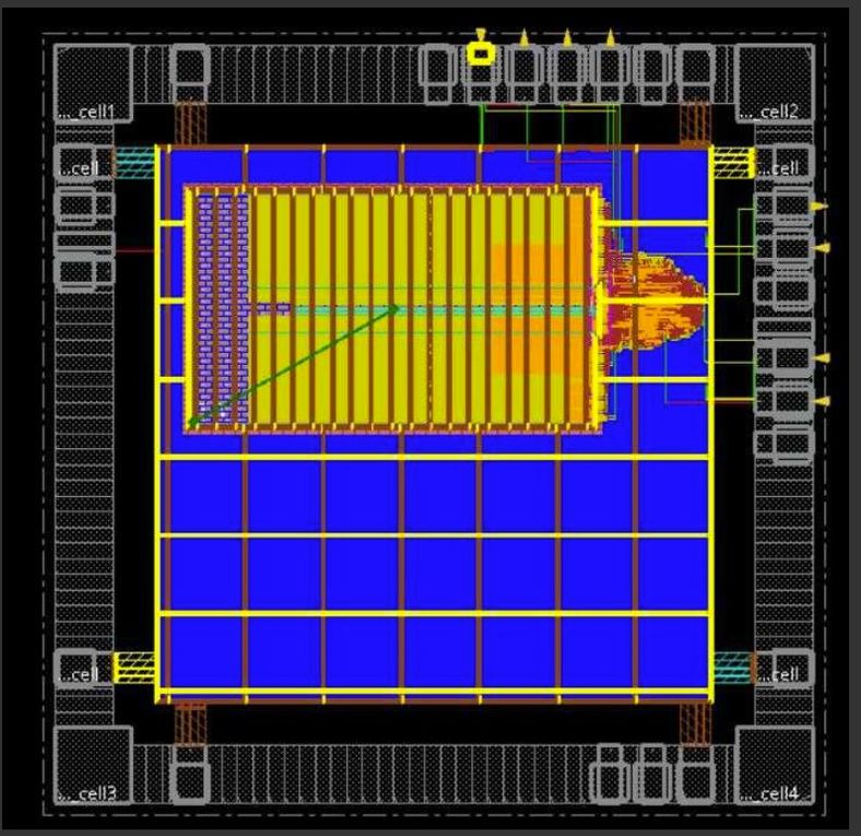
Digital tape-out(Digital ASIC · IL2244 · 2026). Full-chip physical implementation prepared for fabrication.
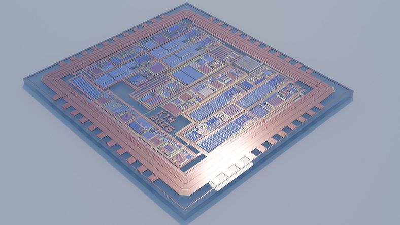
Analog tape-out(Analog IC · KTH · 2026). A complementary analogue design, showing the breadth of hands-on IC design at KTH.
One KTH programme, five university partners
Edu4Chip aligns advanced chip-design education across KTH, TUM, DTU, Tampere University and Institut Mines-Télécom. KTH students can benefit from project-wide activities and complementary expertise at the other partner universities.
- KTH– Stockholm, Sweden
- TUM– Munich, Germany
- DTU– Lyngby, Denmark
- TAU– Tampere, Finland
- IMT– France
View the joint Edu4Chip programme →
Designed for real-world chip development
Edu4Chip connects university education with industrial practice through modern chip-design methods, practical projects, industry interaction and a strong emphasis on employable design skills.
Summer schools and shared activities
Students can take part in Edu4Chip activities organised across the consortium, bringing together students, academics and industry from across Europe. Edu4Chip news and activities →
Contact at KTH
For questions about the KTH implementation of Edu4Chip, the chip-design course pathway, project activities or student participation, contact the KTH project representative:
Prof. Ahmed Hemani
KTH Royal Institute of Technology

Funded by the European Union. Views and opinions expressed are however those of the author(s) only and do not necessarily reflect those of the European Union or European Health and Digital Executive Agency (HADEA). Neither the European Union nor the granting authority can be held responsible for them.