Electron Microscopy Laboratory at KTH Kista
With the complete set of electron microscopy and relevant sample preparation tools in Electron Microscopy Laboratory at KTH, material research has been brought up to an advanced level.
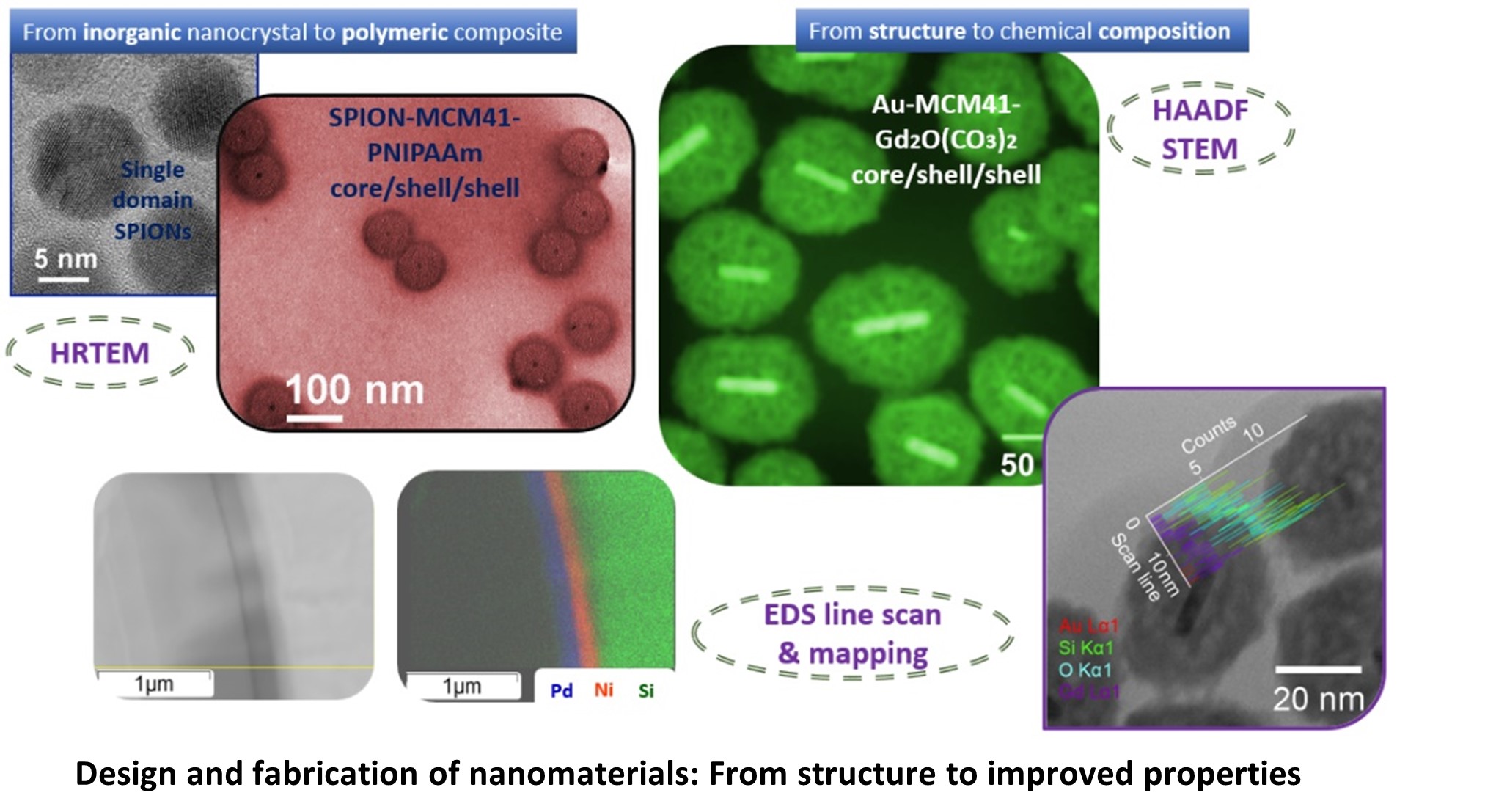
The JEOL JEM 2100F provides atomic level structural analyses in biology, medicine, and materials sciences as well as the semiconductor and pharmaceutical industries, with information on morphology, chemical composition, crystal structure and bonding states of atoms. The JEM-2100F is equipped with STEM, EDS, EELS, and CCD-cameras. Analytical methods include BF-TEM, HAADF-TEM, EF-TEM, ED and EELS. The side-entry goniometer stage provides ease of use tilt, rotation, heating and cooling, programmable multi-point settings-all without any mechanical drift.
The Zeiss Ultra 55 SEM can deliver information on topography, crystallography, and the magnetic field of the sample. It is equipped with large five axes motorized eucentric stage, high efficient In-lens SE detector for high contrast surface imaging, EsB detector for compositional information, ultra-stable high current mode for x-ray analysis (EDS) and EBSD applications. The capability of having multiple detectors makes it a very versatile tool providing valuable solutions for different applications.
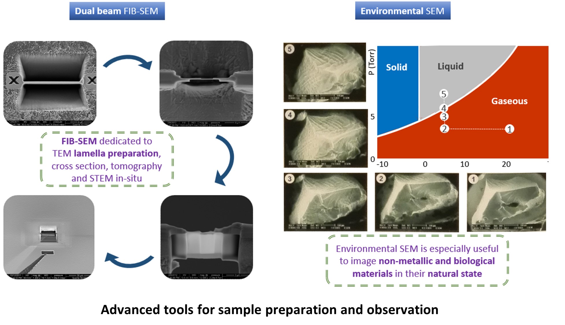
With multiple SE detectors and gas injectors, FEI Quanta 3D FEG FIB-SEM’s unprecedented high-current FIB enables fast material removal and features live SEM imaging while milling. A large selection of gas chemistries is available to deposit materials or further enhancing the FIB milling rate or material selectivity. Automated FIB sectioning recipes enable accurate cross-sectioning, making the FIB-SEM a superior solution for fast preparation of large samples over a wide range of materials.
New materials with superior material functionality, better device performances and advanced manufacturing processes have been identified as the key necessities for achieving a resource and energy sustainable society. The properties of a given material depend on its structure (at different length scales) and composition and thus the fundamental understanding and correlation of these key aspects are the basis of future developments centered on materials. Therefore, structural and chemical information is crucial for scientists and engineers working with materials research where the structure-property relationships are routinely established using imaging, diffraction and spectroscopic techniques where electron microscopy plays an important role. The specialties in Electron Microscopy Laboratory at KTH lie in their expertise in deducing topographic, morphological, compositional and crystallographic information using scanning and transmission electron microscopes (application examples are shown in figures), and skills in effective use of the techniques to generate desired information from a variety of samples, including but not limited to, nanoparticles, mesoporous materials Metal-organic framework (MOF) and Covalent-organic framework (COF), battery and energy materials, catalysts, fiber and cellulose, polymers and composites, metallic materials and alloys, ceramics, semiconductor materials, devices and circuits, magnetic materials and thin films, electron-beam sensitive materials, oxygen/air sensitive materials.