
New dimensions of 3D printing

A drawing programme and a 3D printer: in the future, that’s all it will take to produce customised micro- and nanoscale silicon structures for sensors and other devices.
3D printing is one of the hottest topics in technology, with the potential to revolutionise manufacturing processes in a vast number of fields. And now, in a proof-of-concept project, researchers at KTH EE are taking it down to nanoscale, which could pave the way for cheaper and more accessible manufacturing of customised micro- and nanoscale components in silicon.
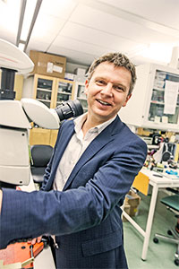
“We have developed a new approach for production of silicon structures for sensors and other devices by combining existing technologies in an innovative way,” says Frank Niklaus, head of the research team and Associate Professor in the Department for Micro and Nanosystems. “Now that we have tested it manually, it can be used as a model for a new 3D printer that can print the sensors.”
Production of silicon sensors at micro- and nanoscale with today’s technologies requires a full-scale clean-room laboratory, which can cost several million euros. These labs are also not suitable for small-scale manufacturing, as the production technology is usually optimised for large production volumes running into hundreds of millions of devices. The new approach developed by Niklaus and his team has the potential to greatly increase the innovation power of both smaller companies and individual researchers and engineers who lack access to expensive semiconductor technology.
Also known as Microelectromechanical Systems (MEMS), these sensors and devices, with accelerometers as one example, are engineered from thin slices of silicon, the same material used to manufacture integrated circuits. MEMS sensors and devices are used in automobiles, in mobile phones for motion control and can also be used in industry and in medical technology.
“These components could be made very easily, flexibly and inexpensively compared with today’s manufacturing processes,” Niklaus says. “All you’ll need is a 3D printer and someone to draw the structure in a drafting programme on a computer.”
The new 3D printing technology consists of an additive layer-by-layer process for defining 3D patterns in silicon, using a focused ion beam followed by silicon deposition. The layered 3D silicon structures are defined by repeating these two steps over and over, followed by a final etching step in which the excess silicon material is dissolved away. In the team’s vision of the future, the structure would first be designed in a 3D drawing programme then sent to a 3D printer that recreates the structure in silicon, layer by layer from the bottom up.
3D printing tools using materials other than silicon — such as polymers, metals, or ceramics — already exist, but they are simply not suitable for micro- and nanostructures, according to Niklaus.
“You really want to use silicon, and that was the starting point for our work,” he says. “We were primarily thinking about using it for sensors, since that is our area of expertise. But it can of course be used for any type of silicon nanostructure.”
Niklaus stresses that the new technology should be seen as a complement to large-scale traditional methods, suitable for volumes up to about 10,000 units.
“For large-scale production, the traditional methodology will always be unbeatable in terms of price per unit,” he says. “But in many applications, when you just want a few thousands units, it is total overkill to use an expensive semiconductor clean-room facility.
“THE NEW method may substantially increase the opportunities for more diversified use of MEMS. It will allow small- and medium-sized enterprises to design MEMS and integrate them into their products much more often, and in a wider range of configurations than at present.”
Drastically reduced production costs will create opportunities for small market innovations, much like dropping computer prices did in the it sector.
“This could allow for manufacturing specially designed sensors for a few patients or creating tailor-made applications for industry at a much lower cost,” Niklaus says. “Giving engineers access to very easy, specialised manufacturing of a diversity of advanced sensors opens up completely new and creative solutions in medical technology.”
In 2011, Niklaus received a grant of EUR 1.5 million from the European Research Council (ERC) for his research on new manufacturing paradigms for micro- and nanosystems. Now he has received an additional EUR 150,000 from the erc to look into the commercial side of the technology, work he will carry out in collaboration with KTH Innovation.
The work done by Niklaus and his team on 3D printing of nanostructures was also recently included in the Watch list of Innovations That Could Change the Way You Manufacture by the Society of Manufacturing Engineers (SME), and will be featured in Manufacturing Engineering magazine and at SME’s 2013 Annual Conference in Baltimore in the US.
Text benny ritzén | Illustrations anders westerberg | Photo Håkan Lindgren