
Novel through-silicon via concept from MST highlighted by industry
An innovative concept for fabrication of through-silicon vias, developed by researches of the KTH Microsystem Lab, was presented as "Top Story" in the Advanced Packaging section of I-Micronews.
I-Micronews, which is related to semiconductor industry technologies is published by Yole Développement, a market research and business development consulting company, facilitating market access for advanced technology industrial projects. Yole Développement is the world leader in the analysis of the MEMS markets: with more than 18 consultants, they are working worldwide with the key industrial companies, R&D institutes and investors in order to help them to understand the markets and technology trends in the MEMS fields.
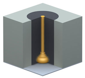
A through-silicon via (TSV) is a vertical electrical connection (via) passing completely through a silicon wafer or die. TSV technology is important in creating 3D packages and 3D integrated circuits.
If you are interested, you can contact us for more information