
3D printers for 2D material research outside the cleanroom
A chemical-and cleanroom-free approach to structure 2D materials
Article abstract:
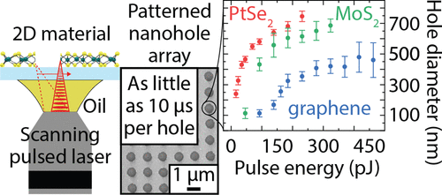
The performance of two-dimensional (2D) materials is promising for electronic, photonic, and sensing devices since they possess large surface-to-volume ratios, high mechanical strength, and broadband light sensitivity. While significant advances have been made in synthesizing and transferring 2D materials onto different substrates, there is still the need for scalable patterning of 2D materials with nanoscale precision. Conventional lithography methods require protective layers such as resist or metals that can contaminate or degrade the 2D materials and deteriorate the final device performance. Current resist-free patterning methods are limited in throughput and typically require custom-made equipment. To address these limitations, we demonstrate the noncontact and resist-free patterning of platinum diselenide (PtSe2), molybdenum disulfide (MoS2), and graphene layers with nanoscale precision at high processing speed while preserving the integrity of the surrounding material. We use a commercial, off-the-shelf two-photon 3D printer to directly write patterns in the 2D materials with features down to 100 nm at a maximum writing speed of 50 mm/s. We successfully remove a continuous film of 2D material from a 200 μm × 200 μm substrate area in less than 3 s. Since two-photon 3D printers are becoming increasingly available in research laboratories and industrial facilities, we expect this method to enable fast prototyping of devices based on 2D materials across various research areas.
Read the full article here:
Ultrafast and Resist-Free Nanopatterning of 2D Materials by Femtosecond Laser Irradiation