
Cutting the cost of micro- and nanomanufacturing
A drawing programme and a 3D printer: that could be all it will take to produce the micro- and nanostructures required for the millions of devices and sensors of the future. With a new manufacturing technology, researchers at KTH Microsystem Technology hope to bring mass innovation capabilities to smaller companies and markets — just as affordable computers have dramatically increased innovation in information technologies.
Production of silicon micro- and nano-sensors with today’s technologies requires a full-scale clean-room laboratory costing millions of euros – facilities that few organisations can afford. What’s more, integrated-circuit manufacturing technologies used in sensor production are highly standardised processes, optimised for extremely large production volumes of hundreds of millions of devices per year. These sensors, known as Micro Electromechanical Systems (MEMS), are engineered from thin slices of silicon, the same material used to manufacture integrated circuits and other micro-sized electronic devices.
Researchers at KTH Microsystem Technology have demonstrated a manufacturing concept that could pave the way toward simple, inexpensive “printing” of 3D silicon structures.
“It could be made very easy, flexible and cheap compared with today’s manufacturing processes. All you’ll need is a 3D printer and someone to draw the structure in a drafting programme on a computer,” says Frank Niklaus, Associate Professor at KTH Microsystem Technology.
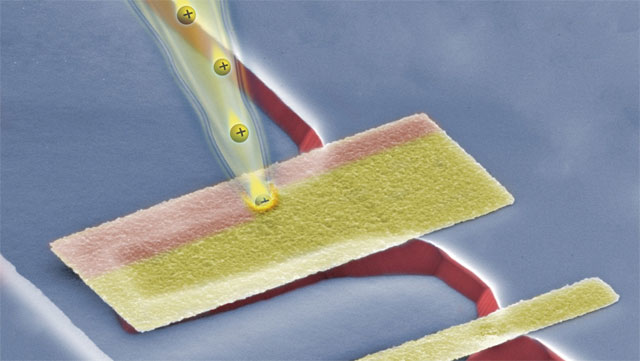
The new manufacturing technology consists of a layer-by-layer process for defining 3D patterns in silicon, using focused ion beam writing followed by silicon deposition. The layered 3D silicon structures are defined by repeating these two steps over and over, followed by a final etching step in which the excess silicon material is dissolved away. The researchers note, however, that the system has so far only been tested manually on relatively simple structures, and that more development lies ahead to implement the concept in a manufacturing tool called a 3D printer.
“In a future manufacturing process, the structure would first be designed in a 3D drawing programme. The drawing is then sent to a 3D printer that recreates the structure in silicon, layer by layer from the bottom up,” explains Niklaus.
In 2011, Frank Niklaus received a grant of EUR 1.5 million (about SEK 15 million) from the European Research Council for his research on new manufacturing paradigms for micro- and nanosystems.
Now the researchers are working to refine the process on a larger scale, and they plan to develop a 3D printer that enables the creation of complex 3D silicon nanostructures. The next step is to commercialise the manufacturing technology in collaboration with partners from industry.
Sensors that detect the orientation and movements of mobile phones or airbag systems in cars are just a few examples of the applications for micro and nano-scale sensors.
“Just imagine all the new applications that people could come up with if they had an easy and cheap way to manufacture nano-structures for sensors and devices. With this tool, we want to enable smaller markets and organisations to advance sensors and other technologies in ways that we can’t even imagine today. I’d compare it to the way affordable computing opened things up for mass innovation in information technologies over the last 30 years or so.”
In June 2012, the team at KTH’s Microsystem Technology Lab and researchers in the university’s laboratories for Engineering Materials Physics and Integrated Devices and Circuits had the results of their research published as an article entitled “3D Free-Form Patterning of Silicon by Ion Implantation, Silicon Deposition, and Selective Silicon Etching” in Advanced Functional Materials, a leading journal in the field.
For more information, contact Frank Niklaus, +46 (0) 8 790 9332, frank.niklaus@ee.kth.se.
Read the scientific paper in Advanced Functional Materials
Text Marie Androv
Edited by Kevin Billinghurst