
KTH to present novel micro and nanosystems at the MEMS2017 conference
The new research will be presented at the 30th IEEE Conference on Micro Electro Mechanical Systems (MEMS) in Las Vegas, USA
The last week of January is the traditional highlight for the Micro Electro Mechanical Systems (MEMS) international research community, as during this time of the year the annual MEMS conference takes place, this year in Las Vegas, USA. Seven innovations from the Micro and Nanosystems department have been peer selected for presentation at this year’s event, with focus on sensing and diagnosis for medical applications, large-scale and versatile nanofabrication methods, and optical communications and sensing.
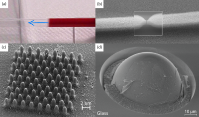
The diagnostic dipstick test format, such as the pregnancy tests, is currently limited in sensitivity and therefore only applicable in a limited number of clinical applications. Variations in clinical sample properties, such as viscosity and surface energy, cause that the output of dipstick tests is limited to yes/no answers. Weijin Guo will present a new dipstick design that makes the device performance independent of the fluid properties of the clinical sample, resulting in more accurate and versatile devices. Similar medical applications can be the outcome of the new fabrication method developed by Reza Z. Shafagh . Reza will present a cheaper and faster fabrication method for replicating plastic structures that include feature sizes in both nanometer and centimeter size. A third innovation, developed by Xiaojing Wang , is a new miniaturised high-energy electron source for generating x-rays for medical applications.
Students Miku Laakso and Valentin Dubois will report on new micro- and nanofabrication approaches. Miku Laakso presents an entirely maskless fabrication concept for manufacturing through glass vias, a key element in high density electronics packaging. The maskless process utilizes laser direct patterning with an ultrashort-pulse laser. This allows fast design improvements, which are ideal for research and product development. Valentin will try to change everyone’s view on cracks. Mostly regarded as a problem, he will present new work showing that tiny cracks can become the long-sought-for solution to make highly relevant nanostructures that are challenging to make even with the most sophisticated tools.
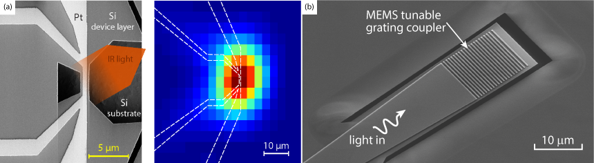
Using micro and nanostructures to emit, control, and detect light has recently enabled new types of sensors and outstanding communication speeds. At the conference, Floria Ottonello Briano will present a very fast and small infrared light detector that can detect weak light signals at room temperature. The detector combines a highly sensitive platinum nanowire with the infrared photonic capabilities of silicon, as well as with its easy and low-cost fabrication. This makes it a cheap and sensitive solution for light detection in sensors. At MST we also use silicon to improve current communication systems by combining traditional optical fibers with on-chip silicon optics. With this application in mind, Carlos Errando-Herranz will present his work on an on-chip silicon device that enables realignment of optical fibers using on-chip silicon optics by simply applying a low voltage, thus solving the very common problem of alignment drift. This simple and low-cost device could increase the lifetime of future high-speed optical communication networks. Also focusing on telecommunications, work by Jonas Hansson on low-cost integration of high-frequency antennas for wireless communication applications will be presented at the conference. They will show how critical microwave components, so called “gap waveguides”, can be manufactured in our previously developed OSTE plastic using a rapid and low-cost method.