
SABIO – nanophotonic biosensors for immunoassays
Ultrahigh sensitivity Slot-wAveguide BIOsensor on a highly integrated chip for simultaneous diagnosis of multiple diseases
2006–2009
In the EU FP6 project SABIO, KTH and the other partners have demonstrated the first optical ring-resonator sensor array integrated fully packaged with a microfluidic network. We have used slot waveguides to achieve a refractive index sensitivity of 246 nm/RIU – the highest reported for a silicon nitride ring-resonator. The system noise level of 1.2 pm, allows a volume refractive index detection limit of 5x10⁻⁶. Refractive Index Units. This is at the time of writing the best experimentally demonstrated detection limit of planar ring-resonator sensors. We have also demonstrated a surface mass detection limit of 0.9 pg/mm2.
The array format of the chip allows measuring several parameters at the same time. This has enabled the thermal compensation technique that was instrumental for achieving the detection limit of 0.9 pg/mm2. The array approach also allows multiple measurement at the same time leading to a more reliable diagnosis and saving of time and money. To our knowledge there are no established label-free IVD devices suitable for multi- detection of peptides, proteins and antibodies on the market.
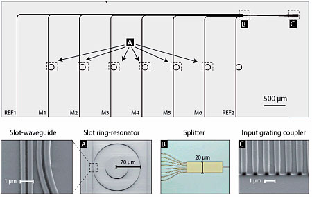
The photonic structures have been fabricated in the KTH cleanroom. They have a waveguide structure in Si3N4 on an SiO2 substrate. This combination offers a good combination of features in terms off compact optical layout, slot waveguide feature size allowing sample access to the slot as well as ease of fabrication and suitable bioreceptor compatibility.
The SABIO device has its own microfluidic system made in polymeric materials for on-chip mass transport. For this we have deviced and tested a novel method for fabrication reliable fluidic vias in a multilayer PDMS system. A novel assembly principle using a dual surface-energy adhesive film was also demonstrated. [More on the sensor in Carlborg et. al., “A packaged optical slot waveguide ring resonator sensor array for multiplex label-free assays in labs-on-chip”, in press, Lab Chip, DOI:10.1039/B914183A, cf. below]
Work performed on the fluidics for the SABIO chip has also allowed us to design, fabricate and demonstrate a microfluidic pumping, dispensing and suction systems, using expandable microbeads as the actuator elements, such as one-time pumps and valves, as well as suction devices. [e.g. Björn Samel, Novel Microfluidic Devices based on a Thermally Resposive PDMS composite, ISBN 978-91-7178-723-3, TRITA-EE2007:31, KTH School of electrical engineering, Stockholm, September 2007, cf. below]
The label-free approach of the SABIO device significantly reduces the efforts and time for the sample preparation process, thus having a simpler and faster whole diagnosis process.
The work on a Hepatitis assay for the SABIO device led to the identification of a novel Hepatitis B antigen variant. This a novel sequence variant of the HBs antigen was discovered by the Medical University of Innsbruck (mutations Q101R, R122I and D144G/G185E), which escapes diagnostic detection and vaccine mediated immunologic protection. This finding has immediate implications for assay licensing and was communicated to the relevant health authorities in Europe and the company Roche (whose platform was used for the development of the immunoassays).
Project impact
Further work in the adaptation of immunoassay procedures for disease diagnosis to the technology developed in the SABIO project opens the door for a diagnosis platform with a huge market potential and application fields.
In vitro diagnosis (IVD) devices have application in multiple fields, not only related with diseases diagnosis, but also with treatment monitoring, drug discovery, environmental control or food security. Thus, market for in vitro diagnosis devices is really wide and plenty of application fields. The future of this market is expected to be the lab-on-a-chip (LoC) devices (as that developed in the SABIO project), where all the mechanisms needed for the immunoassay are integrated in a single chip with reduced size, providing several advantages compared to traditional immunoassay procedures: lower sample preparation effort, higher sensitivity, possibility of performing several immunoassays in a single chip, or lower costs.
The SABIO consortium
Universidad Politécnica de Valencia(Spain) – coordination, biochemistry, optical fabrication
Multitel (Belgium) – measurement setup
Kherion Technologies (United Kingdom) – assay development
Medical University of Innsbruck (Austria) – assay development
Bayer (Schweiz) AG Zweigniederlassung Division Zeptosens (Swiss Confederation) – assay developme
Universidad Politécnica de Madrid (Spain) – optical design
European silicon photonics cluster

A cluster of European silicon photonics R&D projects was formed in April 2010. The projects are funded by European as well as national agencies. The European silicon photonics projects collaborate on dissemination and training activities, and on knowledge and technology transfer from R&D to industry.
European silicon photonics cluster
Silicon Photonics course by the HELIOS project
Project members
Björn Samel
Daniel Hill
Project sponsor
European commission, 6th framework programme
Publications related to this project
- Slot-waveguide biochemical sensor
- Integrated slot-waveguide microresonator for biochemical sensing
- Reconfiguration of microring resonators by liquid adhesion
- Ultrahigh Sensitivity Slot-Waveguide Biosensor on a Highly Integrated Chip for Simultaneous Diagnosis of Multiple Diseases
- Integrated Optical Slot-Waveguide Ring Resonator Sensor Arrays for Lab-on-Chip Applications
- On-chip temperature compensation in an integrated slot-waveguide ring resonator refractive index sensor array