Visa version
Visa
< föregående
|
nästa >
Jämför
< föregående
|
nästa >
Summary; course goals; what is expecting you?
Next scheduled course run: 2014-HT-P2
(autumn term 2014, 2nd period, first course meeting on 3 November 2014 at 10:00 - 12:00 Location: Q11, Osquldas väg 6)
The course is designed as a “hands-on” project course for students who would like to experience the world of nano/microelectromachnical systems (NEMS/MEMS) by having a "hands-on" experience, i.e. by carrying out a microsystem engineering project by designing, fabricating and evaluating tiny but complex devices of sub-millimeter size. This course is given annually, in the 2nd period of every autumn term at KTH (HT-P2; typically last week of October to second week of December).
Course goals:
The students will go through a complete microsystem engineering cycle, as shown in the picture below. Upon completion of the course, they will be able:
- to conceptualize microsystem/microactuator devices for given real-world specifications,
- to model and to simulate microsystems in finite-element (FEM) software,
- to implement designs of microsystems with state-of-the-art CAD design tools into fabrication-ready layouts,
- to fabricate microsystem devices in a state-of-the-art 200-mm wafer semiconductor clean-room laboratory,
- to characterize the performance of microsystem devices, including a comparison of the measured to the predicted performance by the simulations,
- to analyse failure mechanisms and to propose design improvements for a subsequent engineering cycle.
What is expecting you?
Check out the pictures below ...
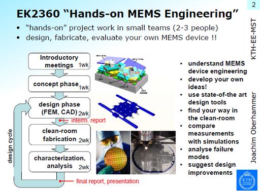
Microsystem Engineering cycle, through which the students will be guided in the course.
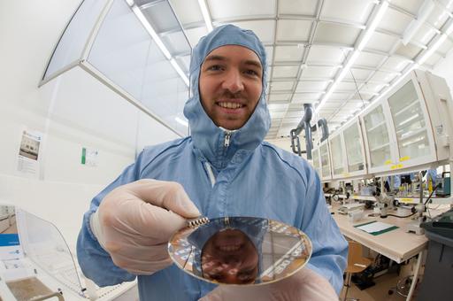
Students (2012 course) fabricating their microsystems in KTH's clean-room. The microsystems are fabricated on such silicon wafers.
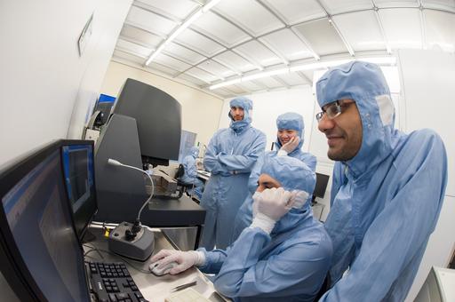
Students (2012 course) in KTH's clean-room during the fabrication part of the microsystems. Here they measure the surface profile of microstructures, to evaluate whether their previous fabrication processes has been successful, before passing on to the next fabrication step.
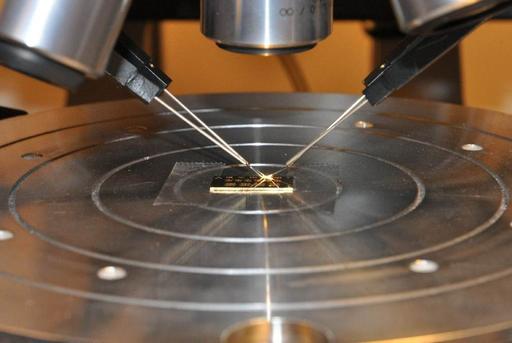
Evaluation of a fabricated chip on a semiconductor wafer measurement probe station (2011 course run). Every student receives such a chip, with his/her own devices and fabricated by himself/herself, as a souvernir after the course.
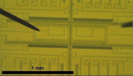
Microscope picture of a microsystem chip fabricated by the students (2011 course run). The probe needles are used for feeding the microsystem actuators with electrical potential, to generate mechanical movements. This chip worked as expected!
For a more detailed description on the course activities, click here.
Return to main course page.